You are using an out of date browser. It may not display this or other websites correctly.
You should upgrade or use an alternative browser.
You should upgrade or use an alternative browser.
Help Please
- Thread starter Mr.Clay
- Start date
.jpg")
No worries we all got to start somewhere....
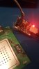
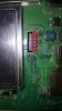
Still wrong on the back pins the you still only have one connected that looks like your black lead that is attached to your GND on the modem , if so that has to be the other end of the back pins ,,,, then you need your TCK which should be the one directly in front of where the black is going to go that has to be moved to where your black lead is currently
Still wrong on the back pins the you still only have one connected that looks like your black lead that is attached to your GND on the modem , if so that has to be the other end of the back pins ,,,, then you need your TCK which should be the one directly in front of where the black is going to go that has to be moved to where your black lead is currently
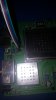
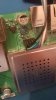
No ,,, you have got the pins on the wrong side again....Look at the picture above and you can see where i showed they must attach too ,,, you are looking at the picure and connecting as you see it ,, but look at the actual layout of your board to see what side is what ,,,, the Red line that is drawn on goes to PIN 1 , you should see a #1 actually printed on the modem PCB
I'm sorry, tbh with you i don't have a single clue what I'm doing, i just brought the flashcatUSB coz i liked what it does, i don't do this stuff, i pentest web and earn money bug bounty sqli injection and all that, so i wanted to try something, new i know this sounds easy for you lot but, i just don't understand once i know what to do i will fly by i Teached my self sql and injection code into we to dump data, so i will teach my self and learn new stuff at this topic but what I'm trying to say the picture don't make sense to me, i can follow like that its hard for me my sound dumb but, i learn my self by reading books n all that stuff really watching Videos. Here i have took a picture of my modem motorolla sb5101e and i have edited i with paint so what side do i have to put the main pins into and what side do i have put the GND.
Attachments
Share: